TSMC’s Bold Move in Chip Packaging
TSMC, a leader in the semiconductor industry, is on the brink of revolutionizing chip packaging to cater to the burgeoning demand for artificial intelligence (AI) chips. In an exclusive reveal by Nikkei Asia, the industry is approaching the final stages of establishing technical standards for an advanced chip packaging technology known as “panel-level”. Anticipated to begin small-scale production by 2027, this advancement marks a significant shift in the semiconductor landscape.
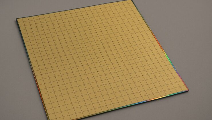
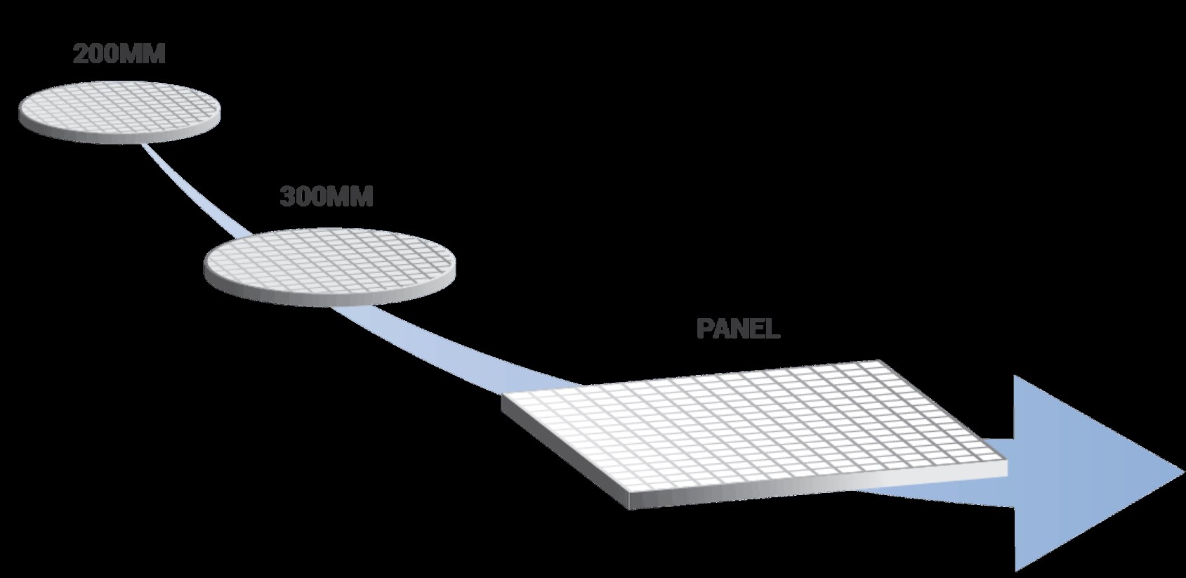
From Round to Square: A Paradigm Shift
Traditionally, chip manufacturing has relied on round 300-millimeter wafers. However, TSMC’s innovative approach will utilize square substrates, with an initial size of 310 mm x 310 mm. Although this size is modest compared to the larger 510 mm x 515 mm panels previously tested, it promises to accommodate more semiconductors than the conventional round wafers. Insiders note that this deliberate choice aims to enhance quality control, particularly addressing the engineering challenge of evenly applying chemical coatings on square surfaces.
Global Implications of the New Manufacturing Technique
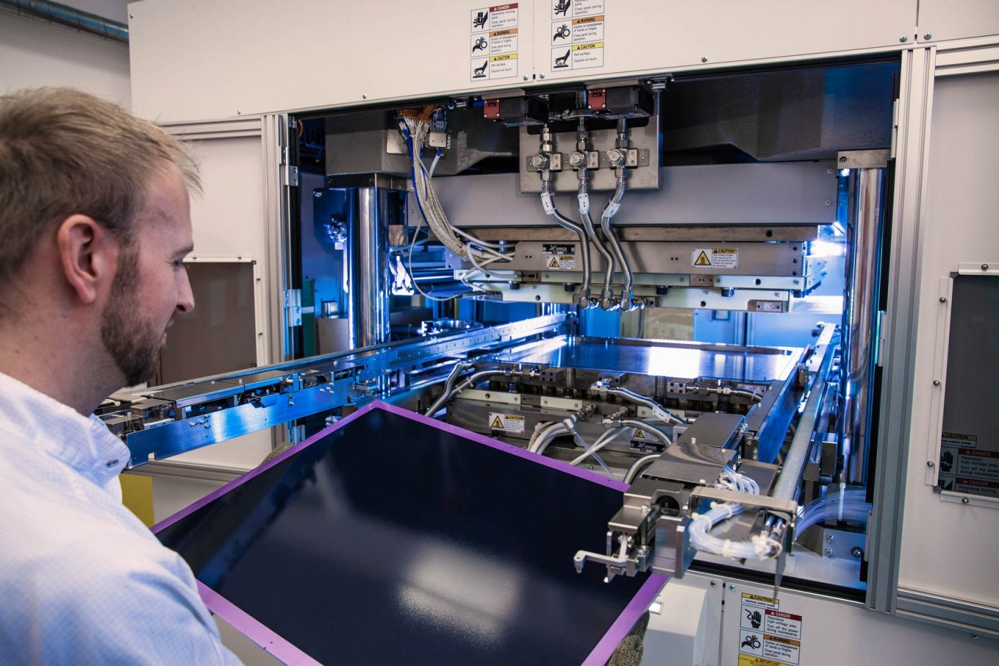
This groundbreaking method is poised to impact not only TSMC but the entire global chip manufacturing ecosystem. Equipment manufacturers hailing from the US, Japan, and Taiwan are already designing new production tools to accommodate these square-shaped bases. Furthermore, handling equipment, including robotic arms, will need adaptation to this novel format. The transition to a square structure is expected to optimize space usage and reduce margins.
To commercialize this technology, TSMC is establishing a pilot production line in Taoyuan, Taiwan, with the ambition to commence limited production by 2027.
The Evolving Importance of Chip Packaging
Historically, chip packaging was viewed as a less sophisticated process compared to chip manufacturing. However, in today’s context, it has evolved into a critical factor determining performance, particularly in AI-specific chips. TSMC’s existing CoWoS (Chip-on-Wafer-on-Substrate) technology is foundational to many advanced systems, supporting innovations from Nvidia’s Blackwell Superchips to solutions by industry giants such as Broadcom, Amazon, Google, and AMD.