
KAPALI
SABAHA KALAN SÜRE


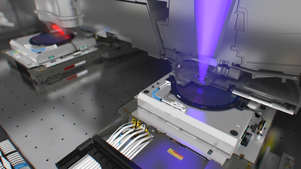

The Japanese state-sponsored chip manufacturer, Rapidus, is gearing up to initiate trial production of its cutting-edge 2nm manufacturing process later this month. As reported by Bloomberg, the company is targeting the completion of its initial test wafers by July, followed by the release of process design kits (PDKs) to facilitate prototyping for initial customers.
Japan’s Semiconductor Advancement Underway
In the latter part of the previous year, Rapidus began outfitting its Innovative Integration for Manufacturing (IIM) facility in Chitose, Hokkaido, with the latest in semiconductor manufacturing technology. This setup includes advanced EUV and DUV lithography systems from ASML. The company is believed to have reached the ‘first light’ stage with these sophisticated tools, signifying its capability to produce circuits using the 2nm process based on Gate-All-Around (GAA) transistor architecture.


Rapidus offers a strategic advantage over industry behemoths like TSMC, Samsung Foundry, and Intel Foundry by aiming to integrate fully automated advanced packaging processes within the same facility. This integration could substantially reduce production times for designs requiring advanced packaging. However, initially, Rapidus will concentrate on wafer production without providing test packaging services.
To enhance its manufacturing processes, Rapidus is establishing a new research and development center named Rapidus Chiplet Solutions (RCS) at Seiko Epson’s Chitose site. Preparations for RCS began in October 2024, with production equipment installation slated for this month. The facility will focus on developing scalable manufacturing techniques, addressing crucial stages such as redistribution layer (RDL) interposer structures, three-dimensional packaging methods, complex assembly design kits (ADK), and QAD (rugged chip) testing processes.
The CEO of Rapidus, Dr. Atsuyoshi Koike, emphasized that the production facilities are advancing as scheduled, with the pilot production line expected to be operational by the end of this fiscal year. The company also aspires to commence mass production of the 2nm process by 2027, aligning its timeline with that of its global competitors.


SİGORTA
6 saat önceENGLİSH
9 gün önceSİGORTA
9 gün önceSİGORTA
10 gün önceSİGORTA
13 gün önceSİGORTA
14 gün önceSİGORTA
15 gün önce
 1
Elon Musk’s Father: “Admiring Putin is Only Natural”
11682 kez okundu
1
Elon Musk’s Father: “Admiring Putin is Only Natural”
11682 kez okundu
 2
7 Essential Foods for Optimal Brain Health
11557 kez okundu
2
7 Essential Foods for Optimal Brain Health
11557 kez okundu
 3
xAI’s Grok Chatbot Introduces Memory Feature to Rival ChatGPT and Google Gemini
11110 kez okundu
3
xAI’s Grok Chatbot Introduces Memory Feature to Rival ChatGPT and Google Gemini
11110 kez okundu
 4
Minnesota’s Proposed Lifeline Auto Insurance Program
9612 kez okundu
4
Minnesota’s Proposed Lifeline Auto Insurance Program
9612 kez okundu
 5
The Division 2: Battle for Brooklyn Expansion
8228 kez okundu
5
The Division 2: Battle for Brooklyn Expansion
8228 kez okundu
Veri politikasındaki amaçlarla sınırlı ve mevzuata uygun şekilde çerez konumlandırmaktayız. Detaylar için veri politikamızı inceleyebilirsiniz.