A New Era in Semiconductor Manufacturing
A groundbreaking advancement is underway in the field of layer alignment, one of the most intricate stages in the semiconductor industry. Scientists at the University of Massachusetts Amherst have unveiled a novel approach that achieves atomic-level precision alignment using lasers and metallenes. As reported by SciTechDaily, this innovation has the potential to transform 3D chip designs and multi-chiplet integrations.
In modern chip fabrication, the process is highly complex, involving thousands of manufacturing steps, particularly for wafers with logic circuits which require approximately 4,000 distinct steps. One of the most crucial aspects is the precise alignment of successive layers – a parameter known as overlay accuracy. Current technologies rely on optical measurement systems, alignment marks, and closed-loop control mechanisms to achieve this. However, these methods face significant challenges, such as a resolution limitation of around 2 to 2.5 nanometers and the inability to simultaneously focus on layers at varying depths. This poses a significant issue, particularly in vertically stacked chip designs.
Innovative Approach with Metallenes and Lasers
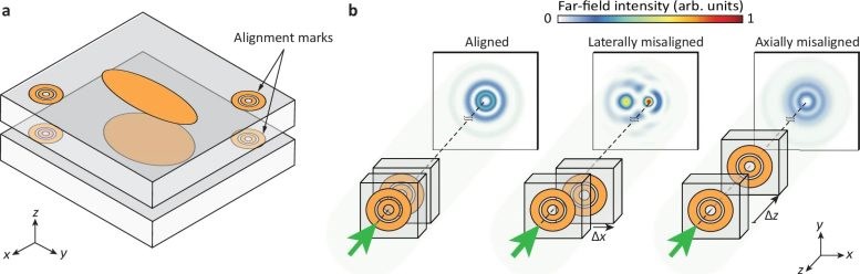
The approach introduced by the UMass Amherst researchers involves placing specially engineered concentric metallenses on the chip’s surface. When these lenses are illuminated by a laser beam, they generate holographic interference patterns. These patterns reveal the direction and magnitude of misalignment between chip layers in three dimensions. Remarkably, this method can detect deviations as minute as 0.017 nanometers horizontally and 0.134 nanometers vertically, surpassing the researchers’ initial target of 100 nanometers sensitivity and exceeding the resolution limits of contemporary optical microscopes.


This method not only promises enhanced precision but also has the potential to decrease production costs by streamlining one of the most intricate steps in chip manufacturing and 3D chip integration. However, like any technological advancement, there are hurdles to overcome. It remains uncertain whether this method can be seamlessly integrated with existing production tools, such as lithography, bonding, and TSV (Through-Silicon Via). If integration proves challenging, the widespread adoption of this innovative technology in semiconductor manufacturing may face obstacles.